暂无评论
图文详情
- ISBN:9787510077869
- 装帧:一般胶版纸
- 册数:暂无
- 重量:暂无
- 开本:24开
- 页数:577
- 出版时间:2014-07-01
- 条形码:9787510077869 ; 978-7-5100-7786-9
本书特色
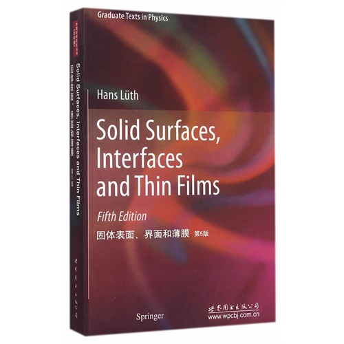
《固体表面界面和薄膜(第5版)(英文版)》讲述固体表面、界面和薄膜的教材已经更新到了第5版,被世界上的众多大学作为教材,可见其经典程度。书中既包含了该科目的理论部分,又包括了实验部分,使其在讲述表面和界面书籍里面具有很强的独特性。书中也提供了基本概念和应用,是学习固态物理的一本**图书。强烈推荐固态物理领域和纳米技术领域的高年级学生和科研人员。
内容简介
这本讲述固体表面、界面和薄膜的教材已经更新到了第5版,被世界上的众多大学作为教材,可见其经典程度。书中既包含了该科目的理论部分,又包括了实验部分,使其在讲述表面和界面书籍里面具有很强的独特性。书中也提供了基本概念和应用,是学习固态物理的一本**图书。强烈推荐固态物理领域和纳米技术领域的高年级学生和科研人员。
目录
1 surface and interface physics: its definition and importance panel ⅰ: ultrahigh vacuum (uhv) technology panel ⅱ: basics of particle optics and spectroscopy problems2 preparation ofwell-defined surfaces,lnterfaces and thin films 2.1 why is ultrahigh vacuum used? 2.2 cleavage in uhv 2.3 ion bombardment and annealing 2.4 evaporation and molecular beam epitaxy (mbe) 2.5 epitaxy by means of chemical reactions panel ⅲ: auger electron spectroscopy (aes) panel ⅳ:secondary ion mass spectroscopy (sims) problems3 morphology and structure ofsurfaces,lnterfaces and thin films 3.1 surface stress, surface energy, and macroscopic shape 3.2 relaxation, reconstruction, and defects 3.3 two-dimensional lattices, superstructure, and reciprocal space 3.3.1 surface lattices and superstructures 3.3.2 2d reciprocal lattice 3.4 structural models of solid-solid interfaces 3.5 nucleation and growth of thin films 3.5.1 modes of film growth 3.5.2 "capillary model" of nucleation 3.6 film-growth studies: experimental methods and some results panel v: scanning electron microscopy (sem) and microprobe techniques panel vi: scanning tunneling microscopy (stm) panei vii:surface extended x-ray absorption fine structur (sexafs) problems4 scattering from surfaces and thin films 4.1 kinematic theory of surface scattering 4.2 the kinematic theory of low-energy electron diffraction 4.3 what can we learn from inspection of a leed pattern? 4.4 dynamic leed theory, and structure analysis 4.4.1 matching formalism 4.4.2 multiple-scattering formalism 4.4.3 structure analysis 4.5 kinematics of an inelastic surface scattering experiment 4.6 dielectric theory of inelastic electron scattering 4.6.1 bulk scattering 4.6.2 surface scattering 4.7 dielectric scattering on a thin surface layer 4.8 some experimental examples of inelastic scattering of low-energy electrons at surfaces 4.9 the classical limit of particle scattering 4.10 conservation laws for atomic collisions: chemical surface analysis 4.11 rutherford backscattering (rbs): channeling and blocking panel viii: low-energy electron diffraction (leed) and reflection high-energy electron diffraction (rheed) panel ix: electron energy loss spectroscopy (eels) problems5 surface phonons 5.1 the existence of "surface" lattice vibrations on a linear chain . 5.2 extension to a three-dimensional solid with a surface 5.3 rayleigh waves 5.4 the use of rayleigh waves as high-frequency filters 5.5 surface-phonon (plasmon) polaritons 5.6 dispersion curves from experiment and from realistic calculations panel x: atom and molecular beam scattering problems6 electronic surface states 6.1 surface states for a semi-infinite chain in the nearly-free electron model 6.2 surface states of a 3d crystal and their charging character 6.2.1 intrinsic surface states 6.2.2 extrinsic surface states 6.3 aspects of photoemission theory 6.3.1 general description 6.3.2 angle-integrated photoemission 6.3.3 bulk- and surface-state emission 6.3.4 symmetry of initial states and selection rules 6.3.5 many-body aspects 6.4 some surface-state band structures for metals 6.4.1 s- and p-like surface states 6.4.2 d-like surface states 6.4.3 empty and image-potential surface states 6.5 surface states on semiconductors 6.5.1 elemental semiconductors 6.5.2 iii-v compound semiconductors 6.5.3 group iii nitrides 6.5.4 ii-vi compound semiconductors panel xi: photoemission and inverse photoemission problems7 space-charge layers at semiconductor interfaces 7.1 origin and classification of space-charge layers 7.2 the schottky depletion space-charge layer 7.3 weak space-charge layers 7.4 space-charge layers on highly degenerate semiconductors ... 7.5 the general case of a space-charge layer and fermi-level pinning 7.6 quantized accumulation and inversion layers 7.7 some particular interfaces and their surface potentials 7.8 the silicon mos field-effect transistor 7.9 magnetic field induced quantization 7.10 two-dimensional plasmons panel xii: optical surface techniques problems8 metal-semiconductor junctions and semiconductor heterostructures 8.1 general principles governing the electronic structure of solid-solid interfaces 8.2 metal-induced gap states (migs) at the metal-semiconductor interface 8.3 virtual induced gap states (vigs) at the semiconductor heterointerface 8.4 structure- and chemistry-dependent models of interface states. 8.5 some applications of metal-semiconductor junctions and semiconductor heterostructures 8.5.1 schottky barriers 8.5.2 semiconductor heterojunctions and modulation doping. 8.5.3 the high electron mobility transistor (hemt) 8.6 quantum effects in 2d electron gases at semiconductor interfaces panel xiii: electrical measurements of schottky-barrier heights and band offsets problems9 collective phenomena at interfaces: superconductivity and ferromagnetism 9.1 superconductivity at interfaces 9.1.1 some general remarks 9.1.2 fundamentals of superconductivity 9.1.3 andreev reflection 9.1.4 a simple model for transport through a normal conductor-superconductor interface 9.2 josephson junctions with ballistic transport 9.2.1 josephson effects 9.2.2 josephson currents and andreev levels 9.2.3 subharmonic gap structures 9.3 an experimental example of a superconductor-semiconductor 2deg-superconductor josephson junction 9.3.1 preparation of the nb-2deg-nb junction 9.3.2 critical currents through the nb-2deg-nb junction 9.3.3 the current carrying regime 9.3.4 supercurrent control by non-equilibrium carriers 9.4 ferromagnetism at surfaces and within thin films 9.4.1 the band model of ferromagnetism 9.4.2 ferromagnetism in reduced dimensions 9.5 magnetic quantum well states 9.6 magnetic interlayer coupling 9.7 giant magnetoresistance and spin-transfer torque mechanism ... 9.7.1 giant magnetoresistance (gmr) 9.7.2 magnetic anisotropies and magnetic domains 9.7.3 spin-transfer torque effect: a magnetic switching device panel xiv: magneto-optical characterization: kerr effect panel xv: spin-polarized scanning tunneling microscopy (sp-stm) problems10 adsorption on solid surfaces 10.1 physisorption 10.2 chemisorption 10.3 work-function changes induced by adsorbates 10.4 two-dimensional phase transitions in adsorbate layers 10.5 adsorption kinetics panel xvi: desorption techniques panel xvii: kelvin-probe and photoemission measurements for the study of work-function changes and semiconductor interfacesproblemsreferencesindex
展开全部
作者简介
Hans Lüth是国际知名学者,在数学和物理学界享有盛誉。本书凝聚了作者多年科研和教学成果,适用于科研工作者、高校教师和研究生。
本类五星书
本类畅销
-

昆虫采集制作及主要目科简易识别手册
¥15.0¥50.0 -

勒维特之星-大发现系列丛书
¥4.0¥16.0 -

昆虫的生存之道
¥11.4¥38.0 -

改变世界的发现
¥16.8¥48.0 -

喜马拉雅山珍稀鸟类图鉴
¥27.9¥68.0 -

中国古代科学思想二十讲
¥12.9¥43.0 -

隐秩序:适应性造就复杂性
¥12.7¥39.8 -

声音简史
¥30.2¥52.0 -

宇宙与人
¥10.5¥35.0 -

星空探奇
¥11.7¥39.0 -

古文诗词中的地球与环境事件
¥8.4¥28.0 -

希格斯:“上帝粒子”的发明与发现
¥14.4¥48.0 -

图说相对论(32开平装)
¥14.7¥46.0 -

走进天文
¥10.5¥35.0 -

现代物理学的概念和理论
¥18.4¥68.0 -

几何原本
¥61.8¥93.6 -

宇宙、量子和人类心灵
¥43.5¥58.0 -

离散数学(第六版)
¥33.9¥49.9 -

自然感悟丛书街巷里的四季:成都草木寻踪
¥33.0¥50.0 -

民国时期机电技术
¥13.5¥45.0


