暂无评论
图文详情
- ISBN:9787030659293
- 装帧:一般胶版纸
- 册数:暂无
- 重量:暂无
- 开本:B5
- 页数:308
- 出版时间:2020-11-01
- 条形码:9787030659293 ; 978-7-03-065929-3
内容简介
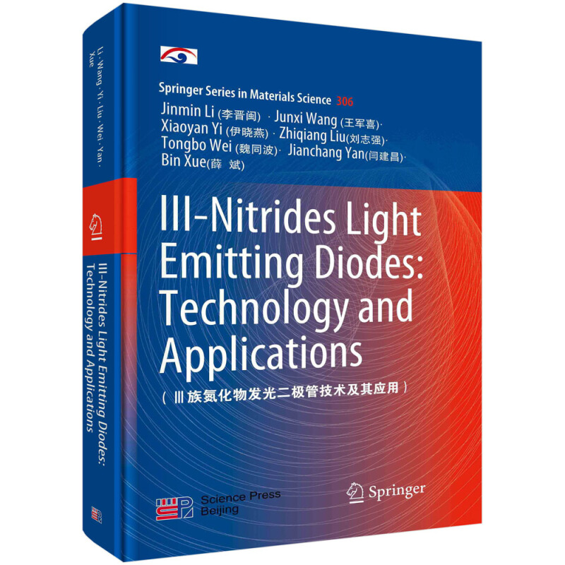
本书以作者及其研究团队多年的研究成果为基础,系统地介绍了Ⅲ族氮化物发光二极管的材料外延、芯片制作、器件封装和系统应用,内容集学术性与实用性为一体。全书共12章,内容包括:Ⅲ族氮化物LED的基本原理、材料性质及外延生长理论,InGaN/GaN多量子阱材料及蓝、绿光LED,AlGaN/GaN多量子阱材料及紫外LED,Ⅲ族氮化物LED量子效率提升技术、关键制备工艺、封装技术及可靠性分析,LED的应用,很后介绍了当前氮化物LED的一些研究前沿和热点。
目录
Contents
1 Introduction 1
References 5
2 Basic Principles of LED 7
2.1 LED Luminescence Principle 7
2.1.1 History and Principle of Lighting Source 7
2.1.2 p-n Junction and the Principle of LED Luminescence 8
2.2 Radiation and Non-radiation Recombination 10
2.3 LED Optical and Electrical Characteristics 11
2.3.1 LED Quantum Efficiency 11
2.3.2 Radiation Spectrum 12
2.3.3 Basic Photometric Concepts in LED 14
2.3.4 Electrical Characteristics of LED 14
2.4 Principle ofWhite LED 15
2.4.1 The Principle of Three Primary Colors and Addition of Light 15
2.4.2 The Realization Method of White LED 15
References 17
3 Properties and Testing of Group III-Nitride LED Materials 19
3.1 Crystal Structure and Band Structure of Group III Nitride 19
3.1.1 Crystal Structure 19
3.1.2 Band Structure 21
3.2 Polarization Effect of Group III Nitride Materials 23
3.2.1 Polarization Effect 23
3.2.2 Influence of Polarization Effect 24
3.3 Doping of Group III-Nitride LEDMaterials 25
3.3.1 Doping of Nitride LEDMaterials 25
3.4 Test and Analysis of the Properties of Group III Nitride Materials 26
3.4.1 Structural and Morphological Analysis 26
3.4.2 Surface and Film Composition Analysis 28
3.4.3 Other Photoelectric Test Methods 30
References 32
4 Epitaxial of III-Nitride LED Materials 33
4.1 Basic Models of Epitaxial 33
4.1.1 3-D Growth Mode (Volmer-Weber Mode) 34
4.1.2 2-D Growth Mode (Frank-Vander Merwe Mode) 34
4.1.3 2-D and 3-D Mixed Growth Mode(Stranski-Krastanob Mode) 35
4.2 Substrate for Epitaxial Growth of III-Nitride LEDs(Sapphire/Si/SiC/LiAlO2/GaN) 36
4.3 Group III Nitride LED Epitaxial Technology 38
4.3.1 LPEMethod 38
4.3.2 MBEMethod 39
4.3.3 MOCVDMethod 39
4.3.4 HVPEMethod 47
4.4 Two-Step Growth Method for MOCVD Grown Nitride Materials 48
4.4.1 Surface Dynamics for Film Growth 48
4.4.2 Two-Step Growth Program for GaN/Sapphire by MOCVD 51
4.5 Influence of Growth Conditions on Epitaxial Layer Quality of Group III NitrideMaterials 53
4.5.1 Effect of Buffer Layer Growth Conditions on Material Quality 54
4.5.2 Effect of Rough Layer Growth Conditions 63
4.6 Epitaxial Technology of High Quality GaN on SiC Substrate 64
4.6.1 Basic Properties of SiC 64
4.6.2 Nucleation and Growth of GaN on SiC Substrate 66
4.6.3 Roots of GaN Stress on SiC Substrates 70
References 71
5 InGaN/GaN Multiple Quantum Wells Materials as Well as Blue and Green LEDs 75
5.1 Introduction to InGaN Material System 76
5.2 Polarization Effects in InGaN/GaN Multiple Quantum WellsMaterials 77
5.2.1 Polarity of GaN-BasedMaterials 77
5.2.2 Spontaneous Polarization and Piezoelectric Polarization 78
5.3 Quantum-Confined Stark Effect 82
5.3.1 Effect on Transition Energy Levels 83
5.3.2 Effect on Luminous Intensity 84
5.4 Carrier Localization in InGaN/GaN Multiple Quantum Wells 84
5.5 Green LED and Non-polar, Semi-polar LED 86
5.5.1 Polar Surface High in Composition Green LEDs 87
5.5.2 Semi-polar and Non-polar Materials 88
5.5.3 Research Progress on Semi-polar and Non-polar LEDs 89
References 90
6 AlGaN-Based Multiple-Quantum-Well Materials and UV LEDs 93
6.1 Introduction of AlGaN Material System 94
6.2 Optical and Electrical Properties of AlGaN Materials 97
6.3 Epitaxial Growth and Doping Techniques for AlGaN Materials 98
6.4 Structure Design and Fabrication of UV LEDs 103
References 108
7 III-Nitride LED Quantum Efficiency Improvement Technology 113
7.1 Three Structures of LED 113
7.2 Internal Quantum Efficiency Improvement Technology 116
7.2.1 Homo-Epitaxial Growth of GaN 116
7.2.2 Multiple Quantum Wells 118
7.2.3 Active Region Doping 122
7.2.4 Electronic Barrier Layer 122
7.3 Light Extraction Efficiency Improvement Technology 124
7.3.1 Patterned Sapphire Substrate 124
7.3.2 Surface Roughening 128
7.3.3 Reflector 130
7.3.4 Flip-Chip Structure 133
7.3.5 Photonic Crystal 134
7.4 Current Injection Efficiency Improvement Technology 134
7.4.1 Current Spreading Layer 135
7.4.2 Current Distribution Theory 136
7.4.3 Current Blocking Technique 140
7.5 Droop Effect 141
7.5.1 Auger Recombination Effect 143
7.5.2 Electronic Overflow 144
References 147
8 III-Nitride LED Chip Fabrication Techniques 151
8.1 Group III Nitride LED Fabrication Process 151
8.2 Photolithography 152
8.2.1 Mask and Photoresist 153
8.2.2 Lithography Process 154
8.3 Etching Process 157
8.3.1 Etching Parameters 158
8.3.2 Wet Etching and Dry Etching 158
8.3.3 Etching of GaNMaterials 159
8.3.4 Etching of ITO and SiO2 Materials 160
8.4 Evaporation and Sputtering 161
8.4.1 Metal Evaporation 161
8.4.2 SiO2 Passivation Layer 162
8.5 Ohmic Contacts 163
8.5.1 n-type GaN Ohmic Contact 163
8.5.2 p-type GaN Ohmic Contact 164
8.5.3 Specific Contact Resistivity 165
8.5.4 Transparent Electrode Technolog
展开全部
本类五星书
浏览历史
-

大学生心理健康教育
¥27.0¥37.5 -

多旋翼无人机控制一体化技术
¥81.9¥130.0 -

Creo6.0工程应用精解丛书Creo6.0运动仿真与分析教程(附光盘)/Creo6.0工程应用精解丛书光盘1张
¥48.5¥69.9 -

破解中小企业融资困境的推进路径探索与内在逻辑研究
¥43.8¥69.0 -

可持续电力系统的建模与控制-面向更为智能和绿色的电网
¥64.4¥88.0 -

清华开发者书库FPGA数字图像采集与处理:从理论知识.仿真验证到板级调试的实例精讲
¥50.7¥69.0 -

高维数据统计学-方法.理论和应用
¥84.6¥95.0 -

运筹学-专业核心课
¥20.8¥36.0 -

体外膜肺氧合技术理论与临床实践
¥112.0¥160.0 -

人格心理学:经典理论和当代研究(原书第6版)
¥81.3¥129.0
本类畅销
-

污水处理工程工艺设计从入门到精通
¥70.3¥89.0 -

发电厂电气部分
¥34.6¥58.0 -

植物进化的故事
¥19.9¥59.0 -

赶往火星:红色星球定居计划
¥44.5¥58.0 -

果脯蜜饯加工技术
¥4.5¥12.0 -

数控车工
¥5.9¥11.5 -

数据驱动的剩余寿命预测与维护决策技术
¥63.4¥79.0 -

手术机器人导航与控制
¥127.4¥169.8 -

射频干扰袖珍手册
¥18.4¥29.0 -

汽车车身构造与修复
¥30.7¥45.0 -

群目标分辨雷达初速测量技术
¥42.4¥69.0 -

秸秆挤压膨化技术及膨化腔流道仿真研究
¥40.6¥55.0 -

NVH前沿科技与工程应用
¥109.7¥159.0 -

电力系统分析
¥23.8¥38.0 -

继电保护原理
¥30.4¥49.0 -

不确定条件下装备剩余寿命预测方法及应用
¥60.4¥99.0 -

船舶分段装配
¥58.6¥80.0 -

基于深度学习的复杂退化系统剩余寿命智能预测技术
¥54.4¥89.0 -

火星探测器轨道动力学与控制
¥59.8¥98.0 -

美军联合作战弹药保障
¥35.8¥58.0
